


NEPCON ASIA 2025 | Unicomp Ra Mắt Kiểm Tra Thông Minh AI + X-quang Thế Hệ Tiếp Theo
2025/10/30

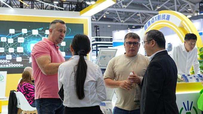
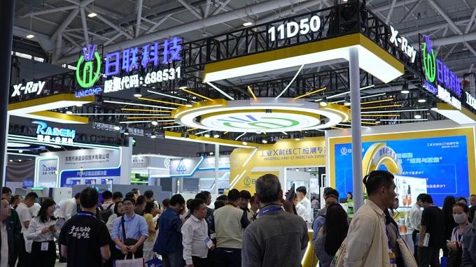
The NEPCON ASIA 2025 triển lãm đã chính thức khai mạc với chủ đề “Hệ sinh thái điện tử thông minh • Cơ hội xuyên biên giới toàn cầu.”
Sự kiện năm nay quy tụ các công nghệ tiên tiến trong lĩnh vực AI, chất bán dẫn và bay ở độ cao thấp, giới thiệu những đổi mới mới nhất trong sản xuất điện tử — mang đến trải nghiệm toàn diện, một cửa cho các chuyên gia trong ngành.

Tại Gian hàng 11, Booth D50, Tập đoàn Công nghệ Unicomp trình bày những đột phá của mình “AI + Kiểm tra thông minh bằng tia X” các giải pháp, nổi bật với hệ thống kiểm tra độ chính xác cao và nguồn tia X tự phát triển giải quyết trực tiếp các thách thức chính trong lĩnh vực chất bán dẫn và điện tử — trao quyền cho khách hàng hướng tới sản xuất thông minh hơn.

Unicomp ra mắt Nguồn tia X loại mở nano-scale 160kV đầu tiên của Trung Quốc!
Thông qua hàng ngàn thí nghiệm và lặp lại quy trình, nhóm R&D của Unicomp đã đạt được một đột phá lớn trong nước — the nguồn tia X loại mở đầu tiên được phát triển hoàn toàn tại Trung Quốc.
Được thiết kế cho ngành công nghiệp bán dẫn, nó cung cấp:
· Độ phân giải cực cao: 0.8 μm
· Khả năng xuyên thấu cao: điện áp ống lên đến 160kV
· Điều khiển thông minh kỹ thuật số: để vận hành ổn định, hiệu quả
Sự đổi mới này giải quyết các nhu cầu kiểm tra khắt khe nhất trong wafer, đóng gói tiên tiến và chip xếp chồng nhiều lớp, thiết lập một tiêu chuẩn mới về độ chính xác nano.
Đối mặt với sự phức tạp của chất bán dẫn — Unicomp giải quyết vấn đề này như thế nào?
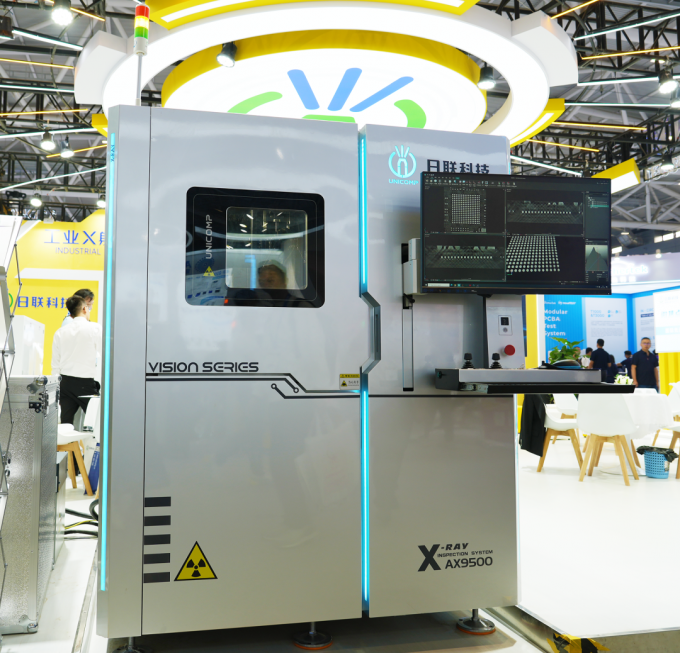
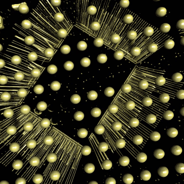
01 ▪ Phát hiện khuyết tật cấp độ Nano
AX9500 | Kiểm tra Nano 3D/CT loại mở
Độ phóng đại 2000X và hình ảnh đa chế độ ghi lại chính xác các khuyết tật như cầu nối wafer, hàn nguội và khoảng trống MEMS, được hỗ trợ bởi mô hình lớn do AI điều khiển để nhận dạng thông minh.
02 ▪ Kiểm soát chất lượng đầu cuối trên dây chuyền bán dẫn/điện tử
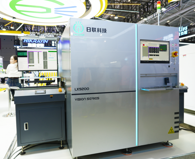
LX9200 AXI | Kiểm tra mô-đun mật độ cao 3D/CT In-line
Được trang bị một nguồn tia X vi mô tự phát triển, nó xuyên qua vỏ hợp kim nhôm hoặc gang 280mm, đạt được Định vị dựa trên AI 360° để phát hiện khuyết tật tự động, chính xác.
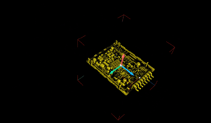
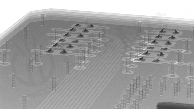
Dòng LX2000 | Kiểm tra tia X In-line độ chính xác cao
Hình ảnh thời gian thực độ phân giải cao ghi lại các khoảng trống và vết nứt nhỏ ở cấp độ micron trong các mối hàn, được hỗ trợ bởi chín thuật toán AI tích hợp để kiểm tra toàn diện tốc độ cao.
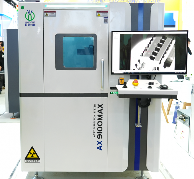
03 ▪ Kiểm soát chất lượng không điểm mù cho các sản phẩm nhỏ gọn, mật độ cao
AX9100MAX | Hệ thống kiểm tra tia X chính xác AI
Được thiết kế cho các cụm điện tử/bán dẫn dày, đặc và lớn, nó tích hợp hình ảnh siêu phân giải dựa trên AI, điều hướng HD, và theo dõi động để phát hiện và theo dõi chính xác các vấn đề về khoảng trống, sai lệch và chiều cao mối hàn.
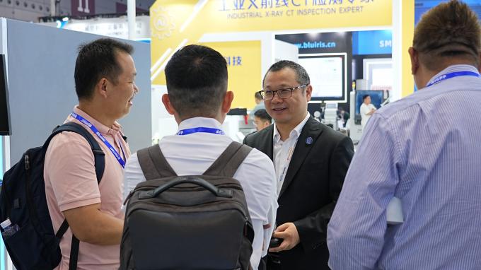
Điểm nổi bật về trao đổi công nghệ
Tại triển lãm, các chuyên gia của Unicomp đã tổ chức nhiều phiên chia sẻ kỹ thuật, thu hút khách tham quan vào các cuộc thảo luận chuyên sâu về cách AI + tia X công nghệ đang xác định lại sự đảm bảo chất lượng bán dẫn và điện tử.
Hướng tới tương lai
Unicomp sẽ tiếp tục phát triển vòng lặp khép kín kiểm tra thông minh AI + tia X, thúc đẩy kiểm soát chất lượng toàn diện và cho phép các ngành công nghiệp bán dẫn và điện tử đạt được năng suất và sản lượng cao hơn — đồng thời.

